This section of FAQs consists of questions realted to CMOS VLSI design issues
What is technology in VLSI?
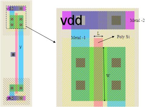
In the context of VLSI technology refers to the feature size, which can be used to implement an integrated circuit. For example when we say the 60 nm integrated circuit technology is used, it means that while making a chip the smallest dimension that is used in making the chip is 60nm. Typically this number is also equal to the smallest channel length possible for MOS transistor. The following figure shows the layout of inverter (taken from electric VLSI design system tool) indicating the Lengh (L) and Width (W) of the MOS transistor.
Why we try to reduce size of transistors?
When we can reduce size of transistors there are several advantages. We improve the speed. We can reduce power consumption. We can reduce the silicon area and hence reducing the cost of the design. Hence when the size of MOS transistor is reduced it is possible to implement design in a lesser cost in low power and high speed.
What is current running Technology in IC Fabrication?
Today several (chip) fabrication centers use 60nm technology for making IC. The 45 nm technology is also available.
What is highly used logic family in chip design today?
Today highly used logic family is CMOS (Complementary metal oxide Semiconductor)
Why Industry prefers CMOS logic family?
The main reason for using CMOS logic family is its low power consumption. CMOS logic family devices only consume power when the device is switching and the power consumption is only the dynamic power consumption the static power component is almost negligible.